 It's already 7 years have passed since we manufactured our first TERS-active cantilevers, - and their characteristics and results constantly grow up and improve all this time. Just recently NT-MDT SI engineers have showed TERS in liquid on an opaque sample, using our cantilevers.
And now we're glad to present the new product - TERS demonstration, - which would be interesting so for new AFM-Raman researchers as for experienced specialists.
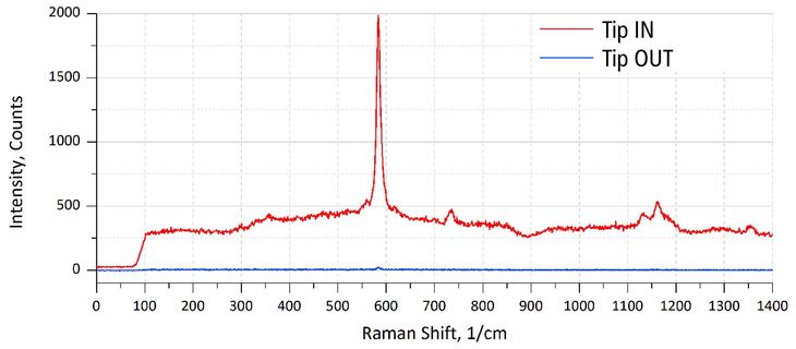
To detect Tip-Enhanced Raman Scattering is a tricky task, which becomes a deal of the independent research for every new type of sample. Before to start such a difficult investigation with the sample targeted it could be reasonable to polish metodology of the experiment with something more simple and reliable. As a starting point the one could took a combination of our TERS-activated cantilevers and specially prepared TERS_S sample. Using this couple experienced engineers from NT-MDT SI get Raman signal enhancement with almost 100% probability.
What could be better to start working with TERS? Only to speak with an experienced AFM-Raman engineer and to see how he gets Raman signal enhancement directly in your lab!
You may find more info about our new product here.
Here at ScanSens GmbH we allways think about how to make recent acheivements in nanoscience more clear and available to everyone. We hope that the new service of TERS demonstration will help our customers to get excellent results in AFM and Raman using other our products, TERS cantilevers and test sample. If any questions appear, please, don't hesitate to contact our sales manager, Evgeniy Lisov (sales@scansens.com).
You're always welcome!
 Besides our wide assortment of AFM cantilevers and silicon grating some other products are also very popular between researchers from various countries. Highly oriented pyrolytic graphite is one of such products. This line of products was started many years ago in the restricted set of thickness and dimensions. From the very beginning we suggested that AFM scientists work with similar sample's holder and our assortment will be just enough to satisfy their needs.
But now we meet very often requests from people, who are not assosiated with scanning probe microscopy at all. HOPG samples application field is very wide due to their structural flexibility and atomic smoothness.
So now, to meet all possible requirements, we decided to broaden our assortment of HOPG samples. We have added several samples of higher lateral size and thickness in all categories from A to H. As usually, you may check the whole assortment at the HOPG and test substrates' part of our web-site.
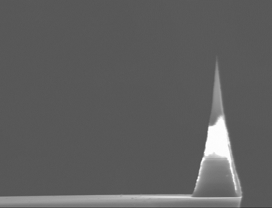 We’re glad to present the new product in our assortment: AFM cantilevers with single crystal diamond (SCD) tips. This type of probes is represented by a very narrow diamond (CVD-grown) needle glued to a standard tipless polysilicon cantilever.
AFM probes prepared by such technology show several features, especially relevant to AFM scans:
 SCD AFM cantilevers are constantly used by famous NT-MDT application scientists: Sergey Magonov and Marko Surtchev. Thus we’re absolutely sure in quality of these probes.
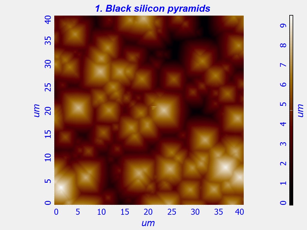
On the right image the one can see a scan of so-called “Black silicon” relief. Such surface can be constructed by a special etching experiment and is used in solar cells.
Main challenges in visualization of “black silicon” pyramids are their heights that reach 6-7 um. Standard cantilever can’t get between such high and densely grown structures. But as the one may see from the scan, SCD probes worked well. Sharp pyramid’s shape and well-defined flat areas between them approve high quality of the scan.
Now SCD cantilevers are presented in our assortment by the models HA_NC/SCD and HA_C/SCD with the same lever’s parameters as for corresponding ones of ETALON series. But by the request SCD needles can be glued to any types of tipless cantilevers of Golden and Etalon series.