For many years ScanSens GmbH works together with experienced engineers in AFM + Raman field. In 2010 our collaboration have resulted in manufacturing the first commercially available reliable TERS-activated AFM cantilevers, based on TOP Visual probes' model.
Since that moment we have constantly worked over improvement of TERS cantilevers' characteristics. Our probes allow to get 100x and higher Raman signal enhancement measuring organic molecules. They were successfuly supplied in many laboratories all over the world, bringing us lots of positive references and sometimes even good ideas for future developements.
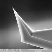
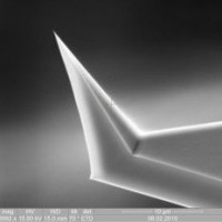
ETALON is a new series of excellent composite AFM probes with two cantilevers on each chip.
|
• Sharp tip (curvature radius less than 10 nm).
• Resonance frequency, specified with high accuracy (±10%).
• Two levers on one chip.
• Special chip geometry for convenient operating.
• High aspect ratio tip.
• Enhanced back-side reflection of the cantilever.
|
|
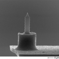
The ETALON Series probe have two polysilicon levers with
a pedestal and monocrystal silicon tips.
Precision technology of polysilicon deposition guarantees the lever thickness control.
A special frequency stabilizer is designed to make the dispersion of the resonant frequency and force constant smaller (due to the lever length control).
Thanks to the above mentioned facts, the ETALON probes are characterized by highly reproducible parameters:
• Typical dispersion of the lever thickness: ±0.15 μm
• Typical dispersion of the lever length: ±2 μm
• Typical dispersion of the probe resonant frequency: ±10%
• Typical dispersion of the force constant: ±20%.
|
 |
Comparison between ETALON and silicon probes
| Parameters | ETALON probes | Silicon cantilevers |
|
Thickness dispersion of the cantilever |
± 0.15 µm | ± 0.5 µm |
|
Length dispersion of the cantilever |
± 2 µm | ± 10 µm |
|
Resonant frequency dispersion |
± 10% | till ± 100% |
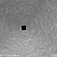
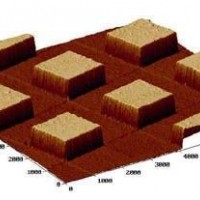
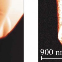
SCAN-GALLERY of the Images obtained by ETALON Probes
 |
 |
 |
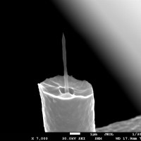
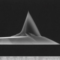
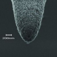
ETALON Premium is the new generation of polysilicon ETALON probes with high reproducible parameters and pencil-shape narrow tips for high quality AFM imaging.
|
Etalon Premium tips have got conical apex and cylindrical body to minimize tip-related widening of objects investigated. Excellent geometry provides high resolution of AFM scans:
|
 |
|
• Sharp tip (curvature radius less than 10 nm).
• Resonance frequency, specified with high accuracy (±10%).
• Two levers on one chip.
• Special chip geometry for convenient operating.
• High aspect ratio tip.
• Enhanced back-side reflection of the cantilever.
|
|
The ETALON Series probe have two polysilicon levers with
a pedestal and monocrystal silicon tips.
Precision technology of polysilicon deposition guarantees the lever thickness control.
A special frequency stabilizer is designed to make the dispersion of the resonant frequency and force constant smaller (due to the lever length control).
Thanks to the above mentioned facts, the ETALON probes are characterized by highly reproducible parameters:
• Typical dispersion of the lever thickness: ±0.15 μm
• Typical dispersion of the lever length: ±2 μm
• Typical dispersion of the probe resonant frequency: ±10%
• Typical dispersion of the force constant: ±20%.
|
|
Comparison between ETALON and silicon probes
| Parameters | ETALON probes | Silicon cantilevers |
|
Thickness dispersion of the cantilever |
± 0.15 µm | ± 0.5 µm |
|
Length dispersion of the cantilever |
± 2 µm | ± 10 µm |
|
Resonant frequency dispersion |
± 10% | till ± 100% |
ScanSens supply with high resolution SPM probes for the main SPM modes.
The probes are supplied with and without reflective coating, with conductive and magnetic coatings to cover the greater part of SPM application range.
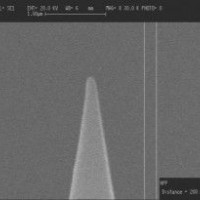
Extremely sharp tips allow to obtain high-quality images of your samples.
Probes have standard chip size that makes them compartible with the devices of the most SPM manufactures.
ScanSens is happy to announce new format of probe puchases. For your convenience we launch new sets which include different probe series for research of different samples by various AFM modes.
UNISETs is the perfect choice for educational purposes or in case you are not sure of the probe type you need for your research and are interested to try different alternatives.
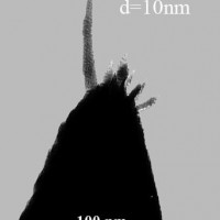
Super sharp silicon probes with typical curvature radius 1-2nm are extremely useful for obtaining high resolution on objects with sizes of several nanometers.
High aspect ratio AFM cantilevers are supposed to be used for obtaining high-quality images of high particles and deep trenches on a surface. Their tip's cone angle is usually less then 10 degrees. That allows a tip to get into narrow gaps between particles making excellent topography detalization. This type of probes is presented in our assortment by two models.
The ideal probe for making AFM Oxidation Nanolithography
Stable and nondestructive,wear resistant probe with conductive diamond coating
allows you to make as many images as you want.
ScanSens offers SNOM aperture cantilevers for contact and noncontact modes.
Company ScaSens manufactures and supplies the full set of calibration standards for SPM lateral and vertical calibration (including submicron calibration in X or Y direction), test grating for determination of the tip shape, SNOM test grating.
Company ScanSens supplies with Highly Oriented Pyrolytic Graphite (HOPG). It's a type of pure, highly laminar graphite used as an atomic-scale calibration standard for atomic force microscopy and scanning tunneling microscopy.
Such HOPG properties as atomic plane surface and good conductivity make it the best material for STM calibration and the excellent substrate for different samples. HOPG is a material that consists of many atomic layers of carbon highly oriented among each other. HOPG is manufactured at the temperature of 3273K and remains stable at the temperatures up to 2000°C in the inert environment. The parallelism of atomic layers is characterized by "mosaic spread angle". The less this angle the higher the quality of HOPG is.
 |
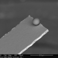
The main features of customized colloidal probes offer:
– 9 standard types of material of colloidal particles are available, the size is variable too;
– Colloidal particles can be attached to almost all the models of commercial tipless cantilevers;
– Colloidal probes with metal coating for conductive AFM measurements are available under request;
– The fixation of colloidal particle can be specially strengthened for friction measurements;
– Special surface modification (for example, hydrophobization) is available under request.
|
| Material type | Diameters available, µm |
| SiO2 | 2.01; 3.5; 4.63; 6.62; 10; 15; 28.75 |
| PMMA | 1.5; 3.36; 6.44; 10; 108 |
| BSG | 2; 5; 10; 20 |
| Gold | 1.5 - 3; 3 - 5.5; 5.5 - 9 |
| Glass beads | 10 - 50 |
| Barium Titanate Solid Glass | 74 - 90; 90 - 106 |
| Soda Lime Glass | 100 |
| Polysterene | 1.98; 3.6; 6.1; 10; 15 |
| Glass | 70 - 110; 180 - 212 |
ScanSens supplies with special colloidal probes for direct surface force measurement, measurement of adhesion forces, study of colloidal interactions between particle and surface and many other applications.