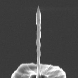
 We're glad to present the new product line in our assortment: Etalon Premium probes with pencil-shape tips for high-quality AFM scanning!
In our experience (and by reports of our customers), these probes show better scanning data for almost all types of surfaces. They are especially effective for high objects of 1 um and higher.
At the moment Etalon Premium probes presented only with HA_NC-based lever parameters. But in the first half of 2019 we plan to expand this product line by HA_C, HA_CNC, HA_FM and HA_HR Premium models. Condutive Etalon Premium cantilevers will be also designed soon.
More detailed technical data can be found on Etalon Premium product page. We hope that our new products will suit well for your investigations!
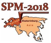 In the end of August together with our colleagues from Ostec-Instruments we were attending International conference Scanning Probe Miscroscopy - 2018 in Ekaterinburg.
We appreciate our colleagues from Ural Federal University - for warm wellcome and excellent organization of all events and lectures, and many interesting people who we met during the conference - for great pastime and valuable ideas for our next developments and common projects.
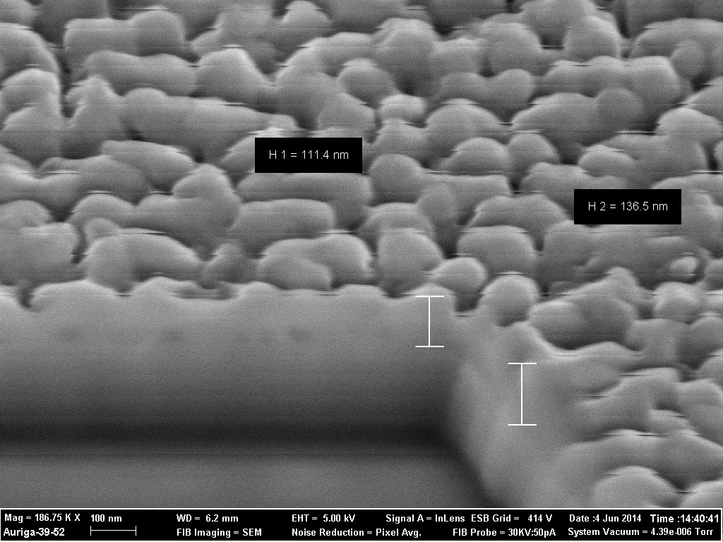 The necessity of tip's shape estimation arises very often during AFM measurements. Even if manufacturer claims this parameter with high accuracy, fast tip's wear off during scanning leads to the need of its repeated re-calculation.
One of the most popular and cheapest methods to control tip's apex is so-called "blind" tip's shape estimation, suggested by J.S. Villarrubia in 1997. Now it is implemented in many different AFM-image-processing programs. But proper choice of a test sample for such investigation is also a tricky task. It should include many densely packed and respectively hard particles, which size will of the same order that tip's curvature radius.
Today we present our new product: TSD01, the test sample for tip's curvature radius estimation. TSD01 consists of large variety of densely packed particles with average diameter around 60 nm. Particles’ shape is not ideally round. Some of them are rather cylindrical, some ones have got vertical walls and sharp corners (like as on the REM photo). These features are necessary to collect enough statistics for further “blind” tip estimation using Deconvolution algorithm.
Another possible usage of this test sample - qualitative tip's quality control by simple comparison of TSD01 scans "before" and "after" scanning.
More information about TSD01 is presented on its product page. We will be also glad to discuss deconvolution method, its possible applications and correct usage of TSD01 for it. Please, contact us if any questions will appear.
 Even full automatic atomic force microscopes are not so easy equipment to deal with. Based on wide and complicated theory of surfaces' interaction AFM method is full of uncertainties. And sometimes only the experienced engineer can say, what does "that artifact" on the image really mean. The one may spend several hours to find the correct parameters... But, according to our experience, sometimes it's enough just to change a cantilever!
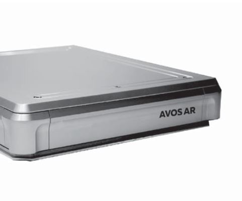 Having many-years experience of work in Atomic Force Microscopy field, we know very well how important good environmental conditions are. And today we're glad to present in our assortment the new product line: vibration control equipment from our partners, Ostec-Instruments.
This product line is really new, and not only for ScanSens. While most of present-day vibration isolation platforms are based on piezo- actuators as active elements, our products utilize electromagnetic coils principle. This progressive technology avoids several problems, such as non-linear response and hard construction, peculiar to piezo- based devices. It allows intelligent integration of a vibration control platform depending on building and environmental properties. The same time specially developed construction provides active isolation in all six degrees of freedom.
Already being sold in several institutes, AVOS platforms have showed excellent vibration protection for various AFM and SEM models. During examination at NT-MDT SI in 2017 the engineer could easily get atomic resolution on Solver NEXT device, placed on AVOS AR module, without any additional protection.
Please, don't hesitate to contact us if any questions will appear. Basing on conditions and possible vibration sources of your laboratory we will be glad to find the best solution that will remove noise from your scans.
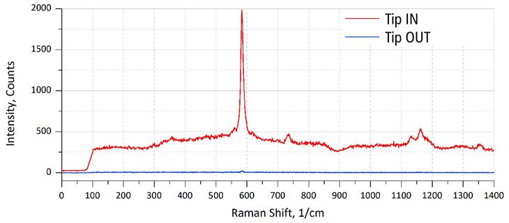 It's already 7 years have passed since we manufactured our first TERS-active cantilevers, - and their characteristics and results constantly grow up and improve all this time. Just recently NT-MDT SI engineers have showed TERS in liquid on an opaque sample, using our cantilevers.
And now we're glad to present the new product - TERS demonstration, - which would be interesting so for new AFM-Raman researchers as for experienced specialists.
To detect Tip-Enhanced Raman Scattering is a tricky task, which becomes a deal of the independent research for every new type of sample. Before to start such a difficult investigation with the sample targeted it could be reasonable to polish metodology of the experiment with something more simple and reliable. As a starting point the one could took a combination of our TERS-activated cantilevers and specially prepared TERS_S sample. Using this couple experienced engineers from NT-MDT SI get Raman signal enhancement with almost 100% probability.
What could be better to start working with TERS? Only to speak with an experienced AFM-Raman engineer and to see how he gets Raman signal enhancement directly in your lab!
You may find more info about our new product here.
Here at ScanSens GmbH we allways think about how to make recent acheivements in nanoscience more clear and available to everyone. We hope that the new service of TERS demonstration will help our customers to get excellent results in AFM and Raman using other our products, TERS cantilevers and test sample. If any questions appear, please, don't hesitate to contact our sales manager, Evgeniy Lisov (sales@scansens.com).
You're always welcome!
 Besides our wide assortment of AFM cantilevers and silicon grating some other products are also very popular between researchers from various countries. Highly oriented pyrolytic graphite is one of such products. This line of products was started many years ago in the restricted set of thickness and dimensions. From the very beginning we suggested that AFM scientists work with similar sample's holder and our assortment will be just enough to satisfy their needs.
But now we meet very often requests from people, who are not assosiated with scanning probe microscopy at all. HOPG samples application field is very wide due to their structural flexibility and atomic smoothness.
So now, to meet all possible requirements, we decided to broaden our assortment of HOPG samples. We have added several samples of higher lateral size and thickness in all categories from A to H. As usually, you may check the whole assortment at the HOPG and test substrates' part of our web-site.
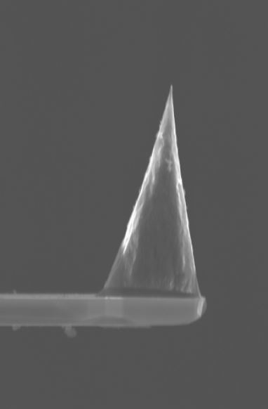
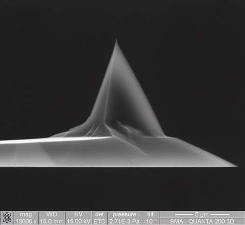
 We’re glad to present the new product in our assortment: AFM cantilevers with single crystal diamond (SCD) tips. This type of probes is represented by a very narrow diamond (CVD-grown) needle glued to a standard tipless polysilicon cantilever.
AFM probes prepared by such technology show several features, especially relevant to AFM scans:
 SCD AFM cantilevers are constantly used by famous NT-MDT application scientists: Sergey Magonov and Marko Surtchev. Thus we’re absolutely sure in quality of these probes.
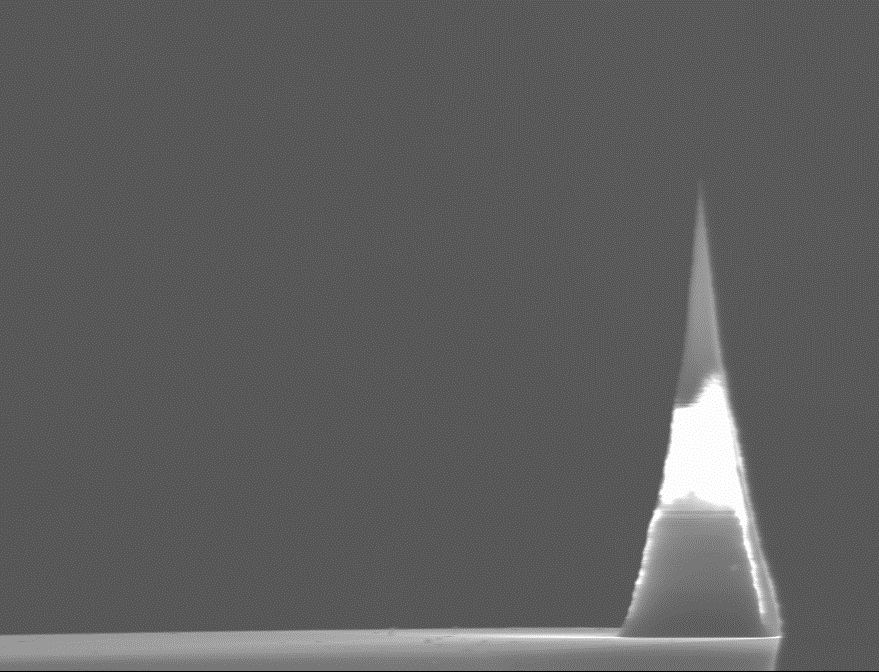
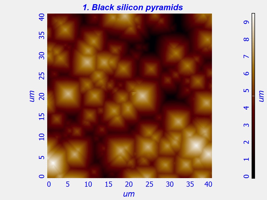
On the right image the one can see a scan of so-called “Black silicon” relief. Such surface can be constructed by a special etching experiment and is used in solar cells.
Main challenges in visualization of “black silicon” pyramids are their heights that reach 6-7 um. Standard cantilever can’t get between such high and densely grown structures. But as the one may see from the scan, SCD probes worked well. Sharp pyramid’s shape and well-defined flat areas between them approve high quality of the scan.
Now SCD cantilevers are presented in our assortment by the models HA_NC/SCD and HA_C/SCD with the same lever’s parameters as for corresponding ones of ETALON series. But by the request SCD needles can be glued to any types of tipless cantilevers of Golden and Etalon series.
 We’re glad to announce that AFM probes with titanium nitride (TiN) coating have appeared in our assortment.
Due to volume doping with anticorrosion elements the new coating W2C+, which was earlier proven to be stable under high currents and pressures, may also work for a long time in high humidity atmosphere.
Several experiments were carried out to check the result. Two sets of probes coated by W2C and W2C+ layers correspondingly were placed into atmosphere of more than 90% humidity for several days. Performance capabilities of the probes were tested by current-voltage curves and scans on HOPG. Before being held in humid air all cantilevers worked correctly showing good conductivity. But already after 8 days old-type coating have lost their conductive properties. The same time probes W2C+ didn’t stop conducting even after 16 days of storage in 90% and more humidity.
We’re also delighted to announce that since June 2016 we will sell only new W2C+ probes from our web-site. The same time, cost of this model stays the same.
More of all, we will be glad if our customers try these probes’ possibilities on practice. When the one orders any model of conductive probes from our web-site this summer we will add to the order a test box of 3 cantilevers HA_C/W2C or HA_NC/W2C at choice.